


In an era of exponential computational growth, optimized verification is no longer merely an advantage—it is a prerequisite. By accelerating the AI/ML-SoC development cycle, innovators can dramatically slash time-to-market and reduce costs, all while securing the performance and energy efficiency required by tomorrow’s complex applications. In short, faster and more secure AI SoC development is essential to meeting the surging demand for more intelligent, efficient, and reliable devices, making it an economic imperative for staying competitive.
The Imperative for High-Performance Verification
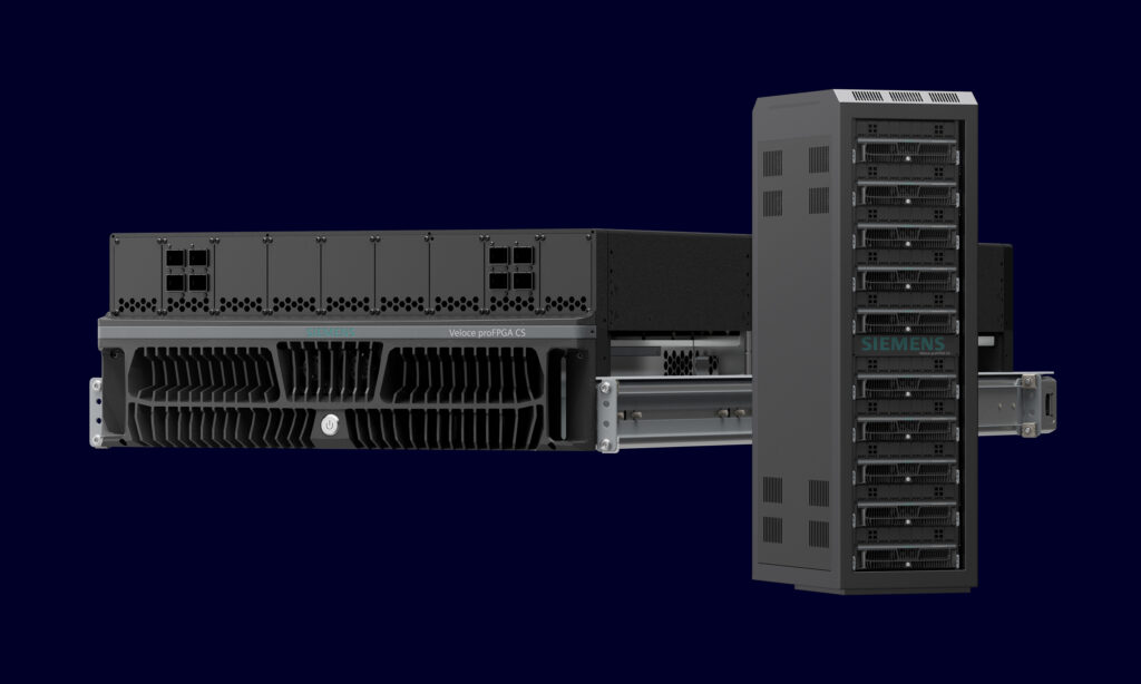
”As AI and computing architectures reach new heights of complexity, semiconductor teams require high-performance verification solutions to validate massive workloads and accelerate time-to-market,” says Narendra Konda, VP of Hardware Engineering at NVIDIA. By integrating NVIDIA’s performance-optimized chip architectures with the Siemens Veloce proFPGA CS, designers can now capture trillions of cycles in a matter of days—delivering the necessary scale to ensure reliability for the next generation of AI.
FPGA-based prototyping systems offer blistering speed, allowing users to execute pre-silicon verification workloads in a fraction of the time required by traditional simulation or even emulation. Yet, modern AI/ML designs are demanding even more, driven by a perfect storm of increasing hardware complexity and ballooning software demands.
Scaling to satisfy rigorous industry demands, accelerated time-to-market targets, and stringent reliability requirements now hinges on the capability to execute trillions of design cycles rapidly. Conventional verification methods, such as simulation and emulation, have reached their limit, unable to scale beyond millions—or, at best, a few billion—cycles within a feasible turnaround time.
The Key Parts of a Pre-Slicon Design Cycle
Finally, a few words about pre-silicon design cycles, which refer to all the development steps that take place before an integrated circuit or chip is physically manufactured in silicon.
Here are the key parts of a pre-silicon design cycle:
* Architecture and specification: You define what the chip will do, its performance goals, and which components are needed.
* RTL design (Register Transfer Level): The design is written in a hardware description language (such as Verilog or VHDL). This is where the ”blueprint” of the chip’s logic is created.
* Verification: The most time-consuming phase. This is where simulations are used to test that the RTL code actually does what it is supposed to do in all possible scenarios.
* Emulation and FPGA prototyping: Special hardware is used to run the design at high speed (but still before manufacturing) in order to start developing software and drivers early.
* Physical Design (Layout): The digital logic is translated into a physical map of how transistors and wires should be placed on the silicon wafer.
* Sign-off: The final check where the design is verified to meet all technical requirements (timing, power consumption, manufacturability) before it is sent to the factory (so-called ”tape-out”).
In short, it is the virtual birth of a chip where software tools are used to ensure that the hardware works perfectly once it becomes reality.

